Physics of
Giga Scale Integration
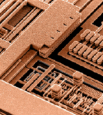
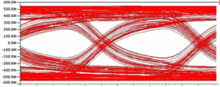
SEM view of 6 levels of IBM Cu interconnect [
ref]
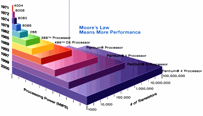
Moore's law has been an important benchmark for developments in
microelectronics for over three decades. Reversing early limitations on
Moore's law, on-chip interconnects have become one of the main
determinants of chip performance. My research interests lie broadly in
modeling and studying problems associated with gigascale integration
(GSI) interconnects at smaller dimensions and higher frequencies. The
solutions to these problems vary from new interconnect-centric design
parigms to the applications of new technologies such as Carbon
nanotubes.
Surface Scattering,
Surface Roughness, Anomalous Skin Effect
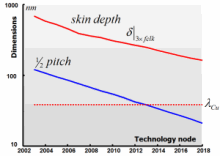
The International Technology Roadmap for Semiconductors projects that
for the year 2018 (18 nm node), interconnects will be as narrow as 21
nm. For a wire with such dimensions, the collision rate of
the electrons with the surfaces will be a significant fraction of the
total number of collisions, causing an increase in the total resistance
of the wire. At the same time, interconnections operate at higher
frequencies, such that electrons are confined to a sheet near the
surface; therefore, the effective cross-sectional area of the conductor
decreases and the effective resistance increases. For a wire that
operates at ultra-high frequencies, such that skin depth and the mean
free path of the electrons are in the same order, skin effect and
surface scattering should be considered at the same time. This is known
as the anomalous skin effect (ASE). My primary research shows that
while ASE has limited impact on delay and bit-rate limit of GSI chips
operated at room temperature, it should be considered for sub-ambient
cooling applications.
Compact Model for
Bit-Rate Limit
As digital circuits approach gigascale integration, the demand for
transmitting data at very high rates grows rapidly. Electrical
interconnects have been conventionally used for on-chip and
chip-to-chip interconnection, and because of the simplicity of the
transmitters and receivers that they need, they will remain an
attractive solution for GSI interconnection. Although electrical wires
are relatively very simple, various effects including surface
scattering and skin effect simultaneously affect their bandwidth, and
make it difficult to accurately determine the bit-rate of electrical
wires. Physical models that accurately determine bit-rate limit of
electrical wires are very helpful in determining their capabilities at
various generations. Such models can also help optimize the
cross-sectional dimensions of wires to maximize aggregate bandwidth.
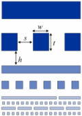
Impact of Size
Effects on the Design and Performance of Metal Interconnect Networks
Size effects have been subject of many studies in the past, and
currently many research groups are investigating techniques that can
potentially mitigate size effects to improve copper conductivity for
the future technology generations. However, a multi-level interconnect
network consists of interconnects with a wide range of lengths that are
routed in metal levels with different pitches and thicknesses. The
impact of size effects on the design of multilevel interconnect
networks has not been studied, and it is not clear how much overall
chip performance will be degraded due to size effects. Such
quantitative analyses can be very helpful for any kind of
cost/performance analysis for various size effect mitigation techniques.
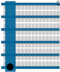
Design and
Optimization for Nanoscale Power Distribution Networks in Gigascale
Systems
As technology advances, it becomes more and more challenging to design
on-chip power distribution networks. This is because, power supply
voltage and hence the noise margin scale down with technology while the
number of devices in a die and the current per unit area of a die scale
up. At the global level, power and ground lines are routed in the top
metal levels with relatively large cross-sectional dimensions, and size
effects do not affect them. At the local level, however, power and
ground lines are routed in the first two metal levels to deliver power
and ground to each individual gate. Due to their small dimensions,
these interconnects are vulnerable to size effects. It is therefore
critical to model and optimize power distribution networks at the local
level and to quantify the impact of size effects on the design and
performance of local power distribution networks.
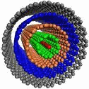
Performance
Comparison between Carbon Nanotube and Copper Interconnects
Carbon nanotubes have received tremendous research interest as they
have many unique mechanical, electrical, thermal, and chemical
properties. A single-walled carbon nanotube (SWCN) is a graphene roll
with a diameter of 0.5 to a few nanometers that, depending on its
chirality, can be either metallic or semiconductor. Multiwall carbon
nanotubes (MWCNs), on the other hand, are concentric graphene tubes
that may have diameters from a few to a hundred nanometers. Copper
wires are facing many challenges as on-chip interconnects, including
their delay, power dissipation, noise, jitter, and electromigration.
Carbon nanotubes can potentially address these challenges if they are
optimally utilized.